
Scanning electron microscopes Sigma
FE-SEM for High-Quality Imaging & Advanced Analytical Microscopy
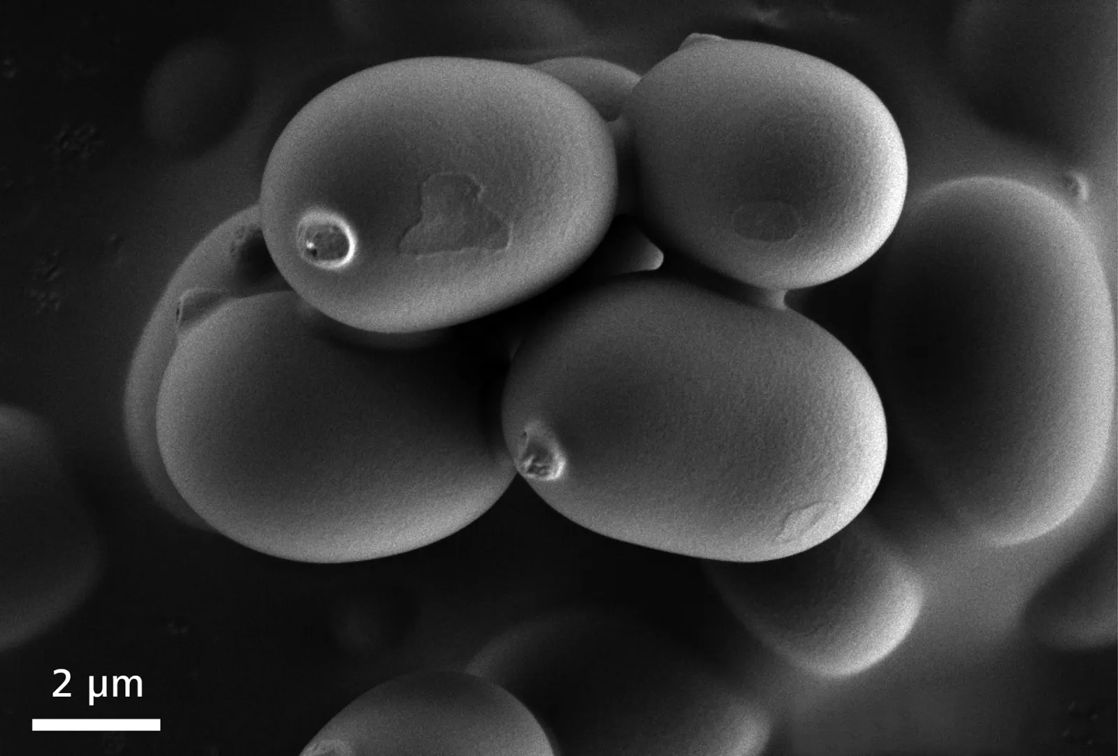
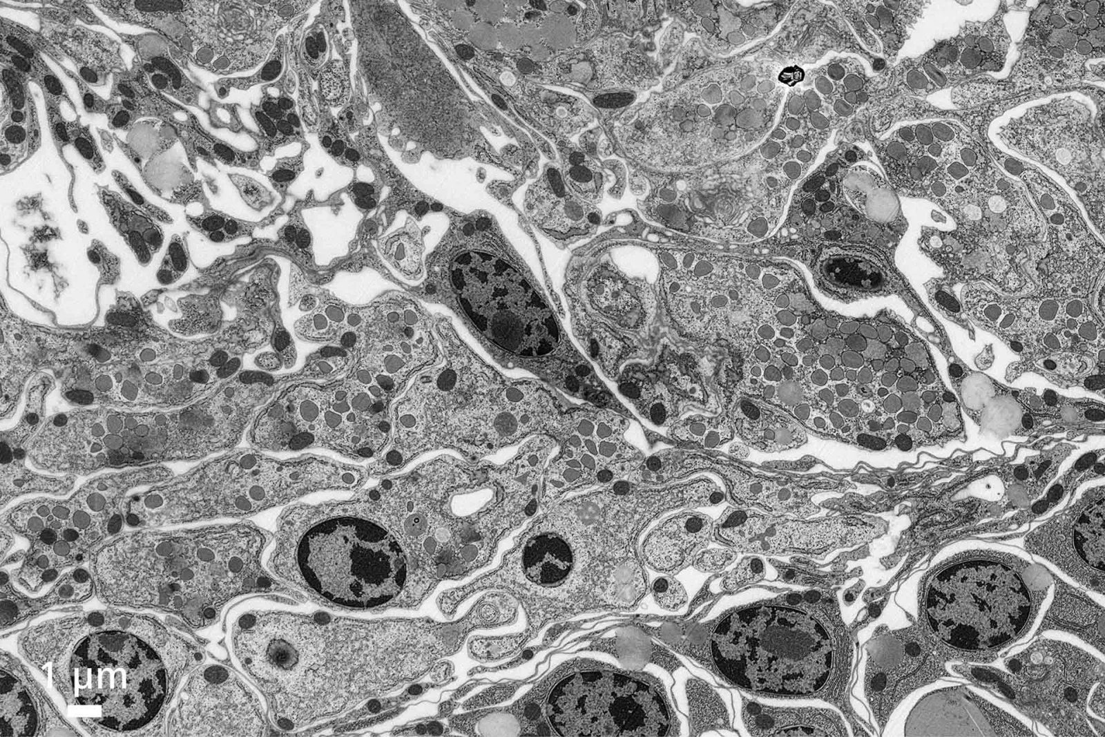
The ZEISS Sigma family combines field emission scanning electron microscope (FE-SEM) technology with an excellent user experience. Structure your imaging and analysis routines and increase productivity. Study new materials, particles for quality inspection or biological or geological specimens. Make no compromises in high resolution imaging – go to low voltages and benefit from enhanced resolution and contrast at 1 kV or below. Execute advanced analytical microscopy using best-in-class EDS geometry and get analytical data at twice the speed and with more precision.
With the Sigma family you are entering the world of high-end nano-analysis.
- Sigma 360 is the core imaging facility’s choice — an intuitive FE-SEM for imaging and analytics.
- Sigma 560 uses best-in-class EDS geometry to deliver high throughput analytics and enable automated in situ experiments.
Sigma 360
The Core Facility’s Choice. Intuitive Acquisition.
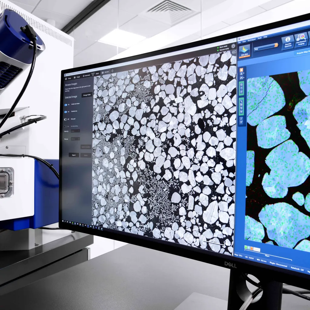
- Be guided expertly from setup to AI-based results. Discover an intuitive imaging workflow.
- See the difference at 1 kV and below. Achieve enhanced resolution and optimized contrast.
- Perform VP imaging at the extremes to achieve excellent results on non-conductors.
An Intuitive Imaging Workflow Guides You
From Setup to AI-based Results
- Get expert results even if you’re a novice user. Benefit from fast time-to-image and save time on training with an easy-to-use, easy-to-learn workflow that lets you streamline each step from navigation to post-processing.
- Software automation in ZEISS SmartSEM Touch starts you off with navigation, parameter setup and image acquisition.
- Then ZEN core comes into play: it comes with task-specific toolkits and is optimally suited for post-processing. The most recommended ones are: The AI Toolkit lets you segment images based on machine learning. Combine multi-modal experiments with the Connect Toolkit. Or use the Materials Apps to analyze microstructure, grain size or layer thickness.
See the Difference at 1 kV and Below
Enhanced Resolution. Optimized Contrast
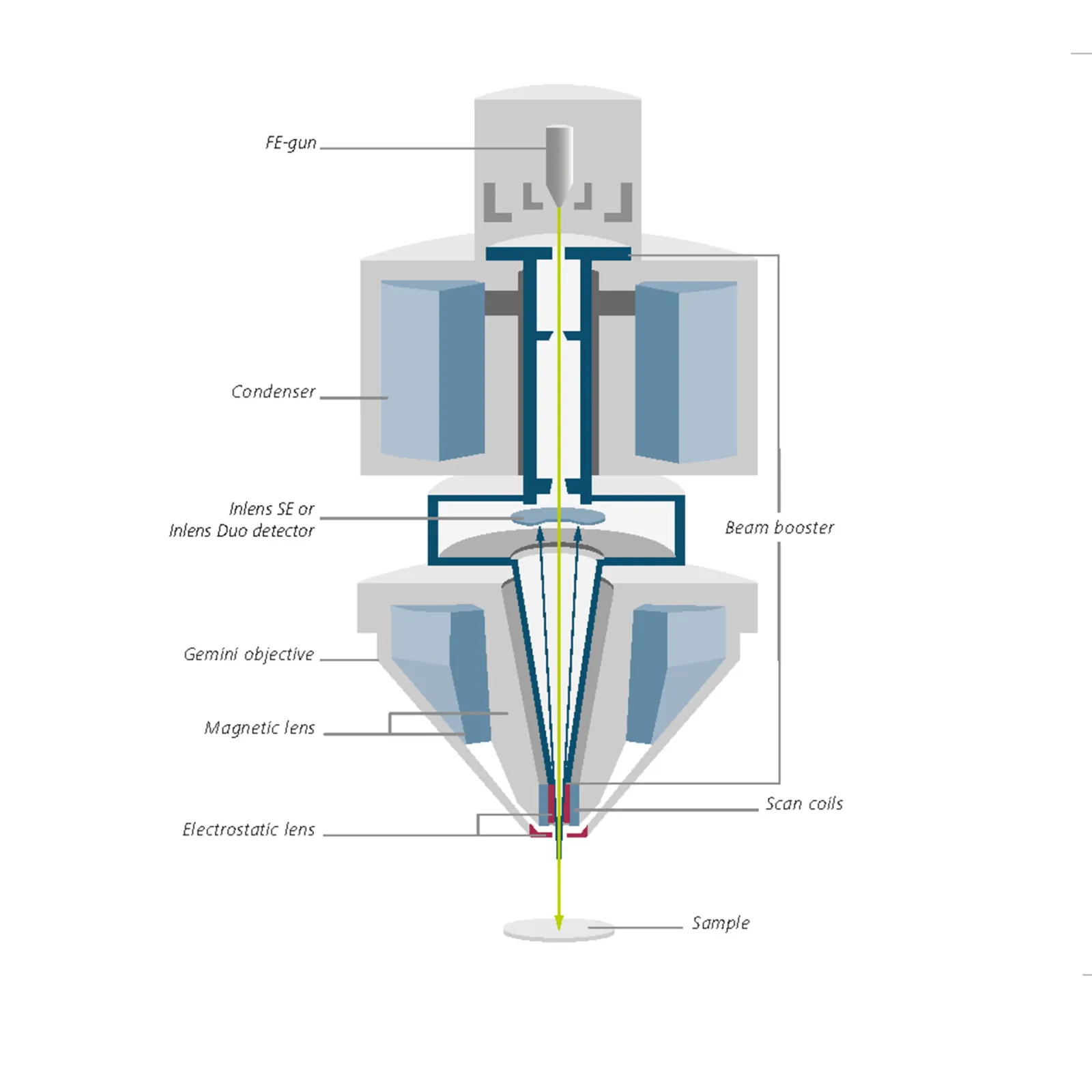
- The optical column is key to performance in imaging and analytics. Sigma operates with ZEISS Gemini 1 electron optics which provide excellent resolution on any sample, especially at low voltages.
- Low-kV resolution for Sigma 360 is now specified at 500 V with 1.9 nm. An improvement in 1 kV resolution of more than 10%—at 1.3 nm—has been achieved by minimizing chromatic aberrations.
- Imaging is now easier than ever before, even on challenging samples, even with backscatter detection in variable pressure (VP) mode.
Accomplish VP Imaging at the Extremes
NanoVP lite Mode for Analytics and Imaging
- The new NanoVP lite mode and new detectors make it easy to achieve high-quality data from non-conductors below 5 kV.
- Consequently, imaging and EDS analytics are enhanced and deliver more surface-sensitive information, faster acquisition times and enhanced primary beam current for faster EDS mapping.
- New detectors such as the aBSD1 (annular backscatter electron detector) or the next generation C2D (cascade current) give you the benefit of excellent images at low voltage.
Sigma 560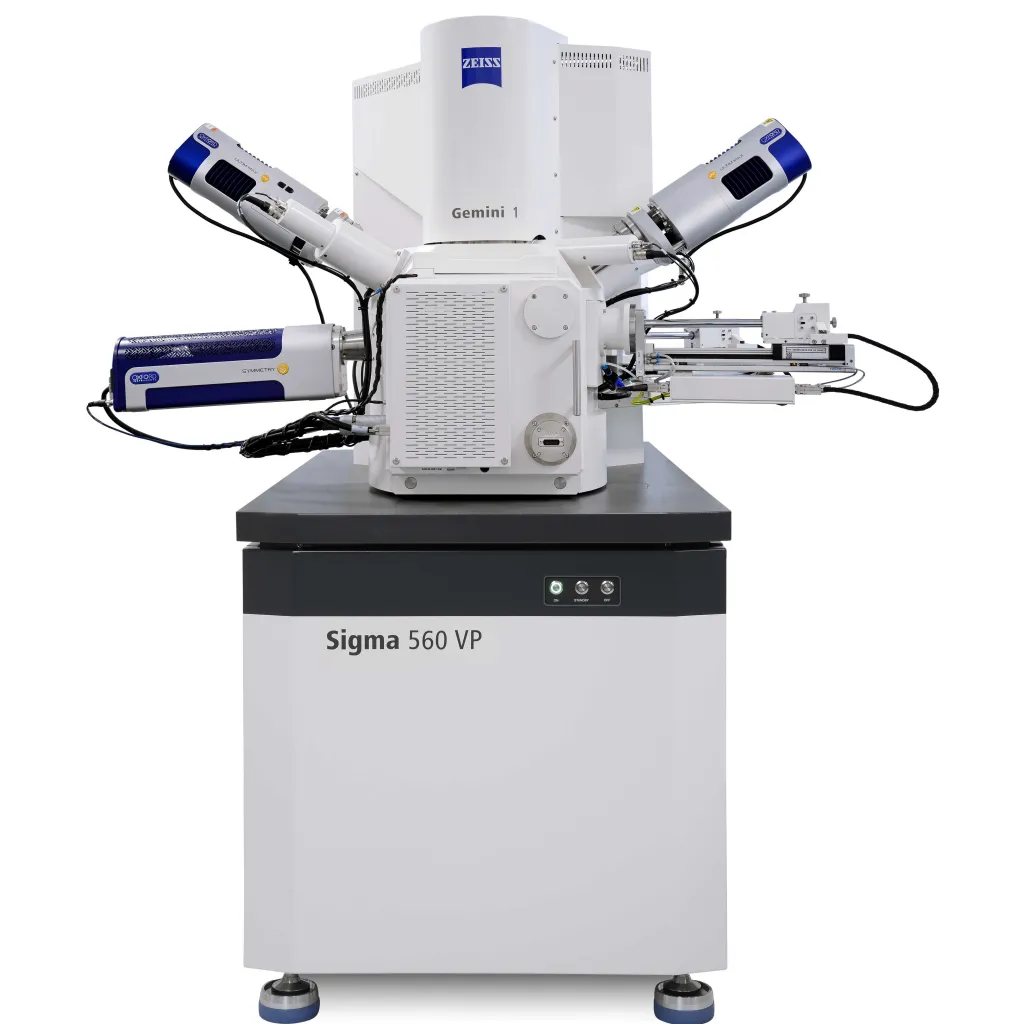
High Throughput Analytics. Automated in situ Experiments.
- Efficient analytics of real-world samples: SEM-based analyses with speed and versatility.
- Automate your in situ experiments: A fully integrated lab for unattended testing.
- Image challenging samples below 1 kV: Collect comprehensive sample information.
Image Challenging Samples Easily
See the Difference at 1 kV and Below
- Achieve best informative imaging and analysis at 1 kV or even 500 V: low-kV resolution for Sigma 560 is specified as 1.5 nm at 500 V.
- Investigate challenging samples easily under variable pressure in the new NanoVP lite mode, with acceleration voltages as low as 3 kV, using either the new aBSD or C2D detector.
- If you are studying electronic devices, you will want to maintain a clean environment. Protect your chamber from contamination by means of a (highly recommended) plasma cleaner, and with the new large airlock that permits shuttling of 6” wafers.
Efficient Analytics of Real-world Samples
Investigate with Versatility and Gain Speed in EDS
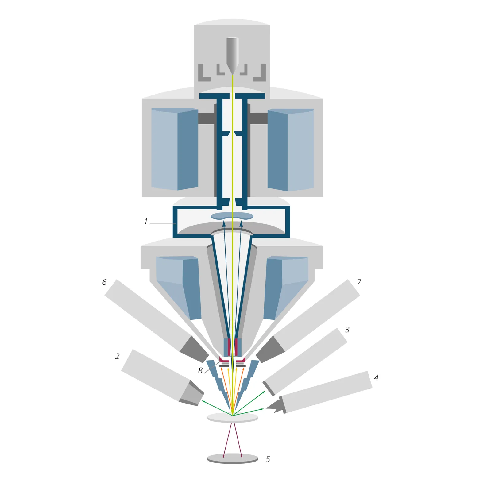
- Sigma 560’s best-in-class EDS geometry increases your analytical productivity. The two 180° diametrically-opposed EDS ports guarantee throughput and shadow free mapping, even at low beam current and low acceleration voltage.
- Additional ports for EBSD and WDS on the chamber allow for analytics beyond EDS.
- Even non-conductors can be analyzed with the new NanoVP lite mode with more signal and contrast.
- The new aBSD4 detector delivers images on highly topographical samples easily.
Automate Your in situ Experiments
- The in situ lab for Sigma, a fully-integrated solution, enables operator-independent results of heating and tensile tests in an unattended, automated workflow.
- Extend your workflow further by analyzing nano-scaled features in 3D: perform 3D STEM tomography or execute AI-based image segmentation.
- The new aBSD4 permits live 3D surface modeling (3DSM)
Technology
Gemini 1 Optics
Flexible Detection
NanoVP lite Mode
- In NanoVP lite the skirt effect and the beam gas path length (BGPL) are reduced. The reduced skirt leads to an enhanced signal-to-noise ratio in SE and BSE imaging.
- The retractable aBSD with its five annular segments delivers excellent material contrast: it carries the beam sleeve and is fitted under the pole piece during NanoVP lite operation. It provides high throughput and low voltage compositional and topographical contrast imaging and is suitable for VP and HV (high vacuum).
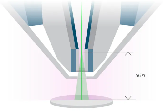
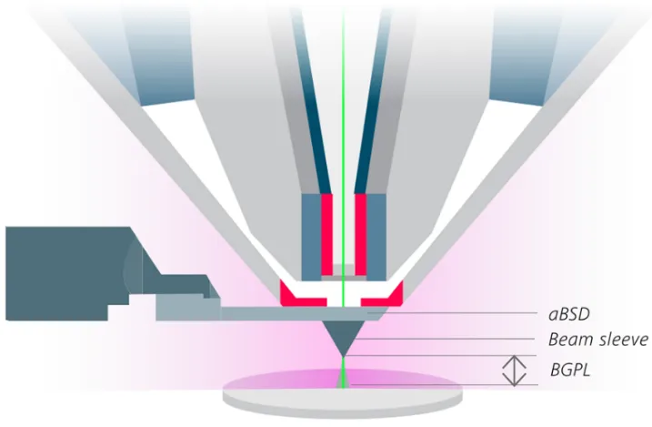
Standard VP (left) and NanoVP lite (right) modes, gas distribution (pink), electron beam skirting (green).
Materials Science
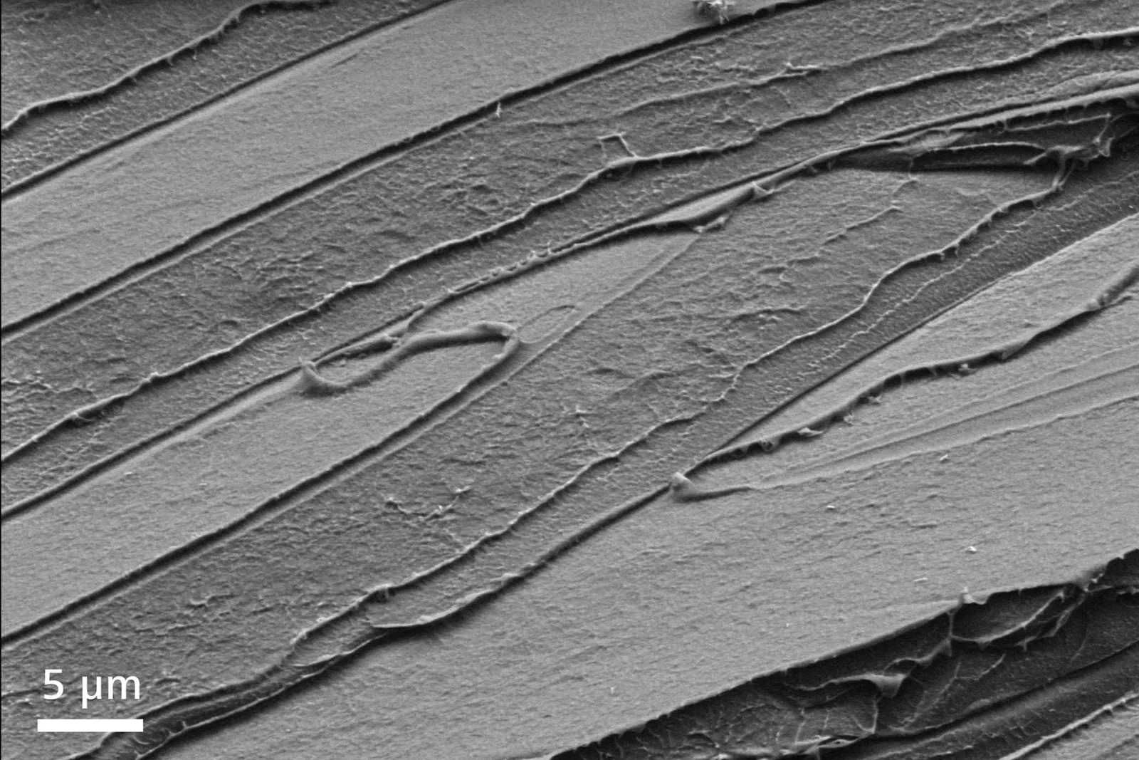
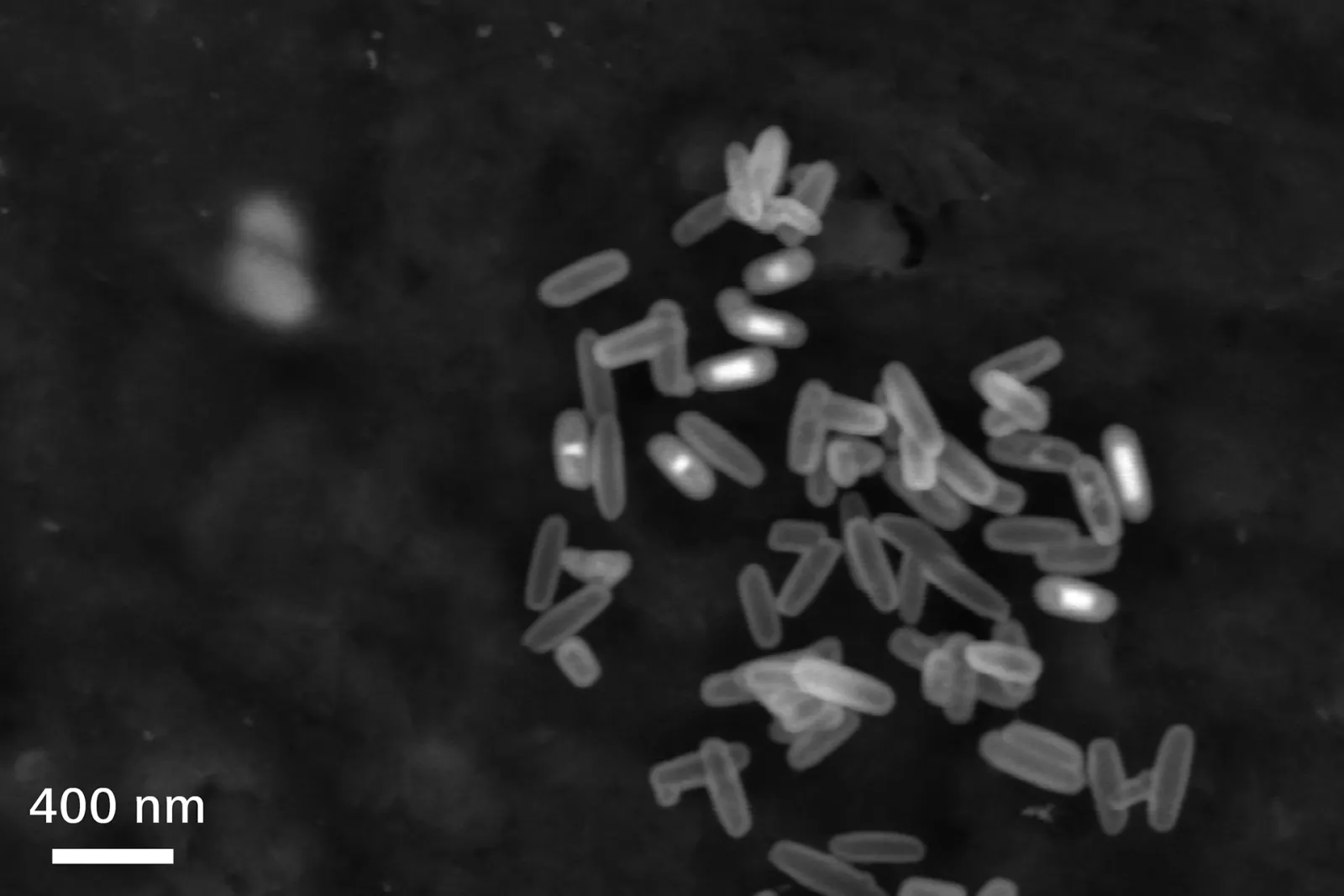
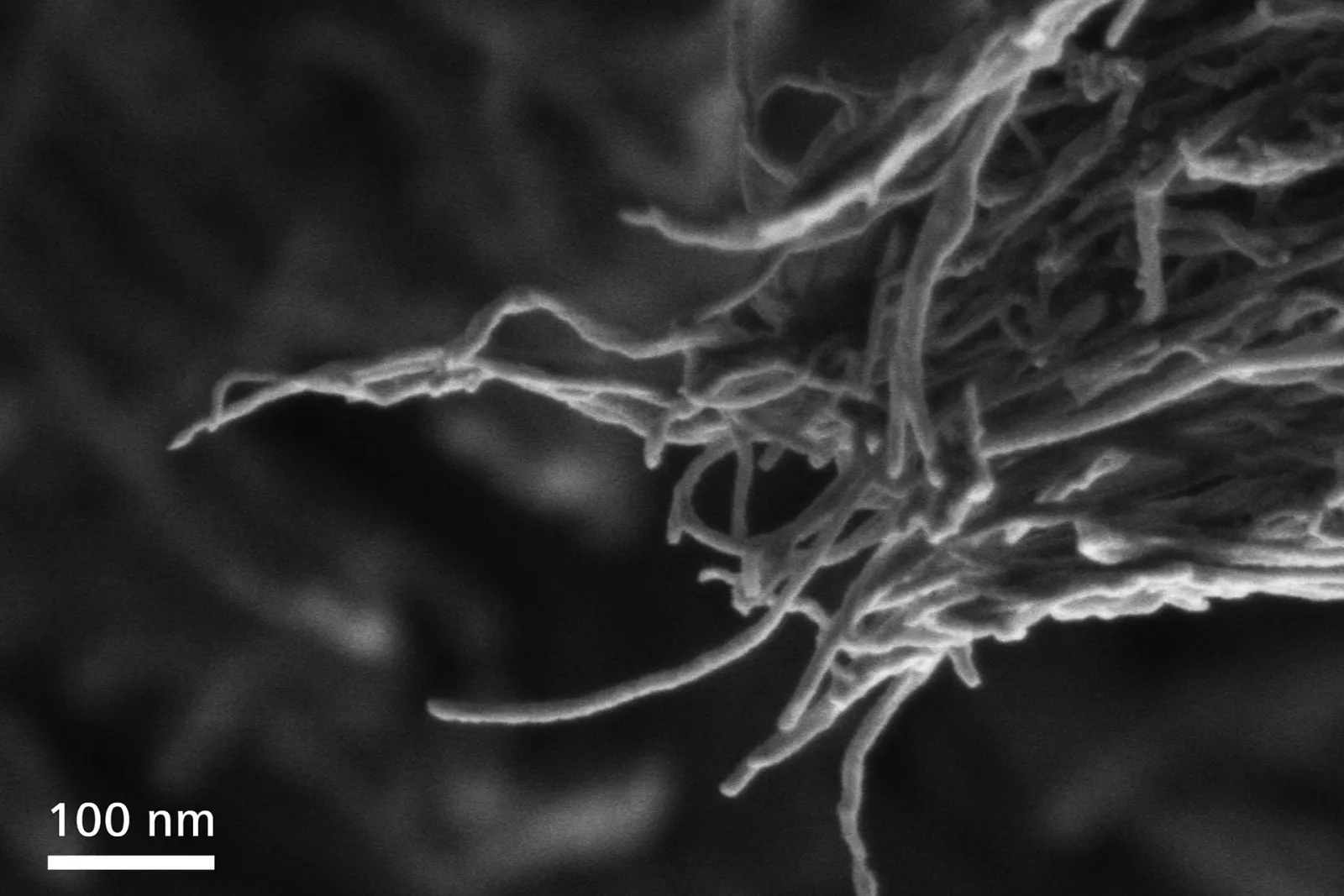
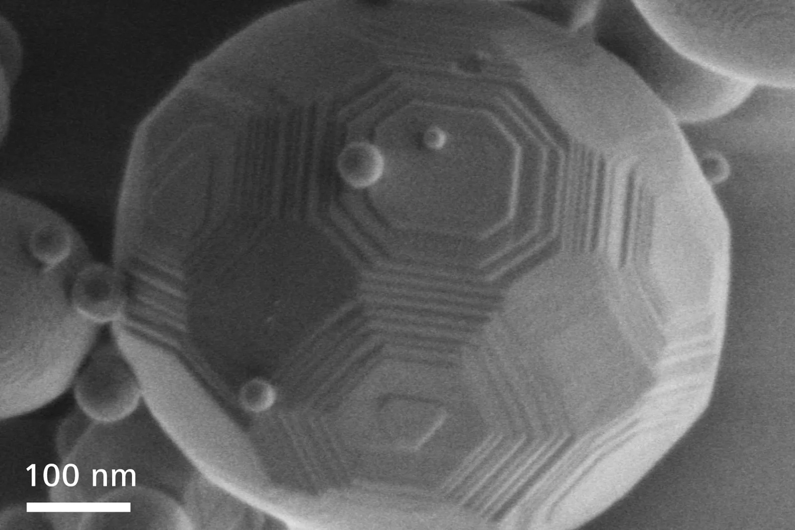
Discover images of materials samples such as polymers, fibers, molybdenum disulfide and more.
Life Sciences
Learn more about of the micro- and nanostructure of protozoans or fungi and reveal ultrastructure on block face samples or thin sections.
