

Scanning electron microscopes GeminiSEM
FE-SEM For Highest Demands in Sub-nanometer Imaging, Analytics and Sample Flexibility
ZEISS GeminiSEM stands for effortless imaging with sub-nanometer resolution. These FE-SEMs (field emission scanning electron microscope) combine excellence in imaging and analytics. Innovations in electron optics and a new chamber design let you benefit from better image quality, usability and flexibility. Take sub-nanometer images below 1 kV without an immersion lens. Discover three unique designs of the ZEISS Gemini electron optics.
- Ideal for core facilities - ZEISS GeminiSEM 360
- Enabling efficient analysis - ZEISS GeminiSEM 460
- New standard for surface imaging – ZEISS GeminiSEM 560
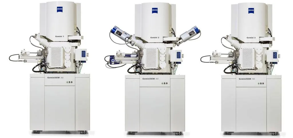
GeminiSEM 360
GeminiSEM 360 is the ideal instrument for your core facility, delivering maximum versatility for materials & life science, and industry. With its Gemini 1 electron optical column it delivers high resolution imaging and analytics over the widest range of applications and sample types.
Benefit from surface sensitive imaging and gather information at low voltage or at high probe current. Discover the advantages of Inlens detection, NanoVP, contextual image viewing or AI-powered segmentation.
- Your tool for sample flexibility
- Unrivalled user experience
- Exceptional capability extension
GeminiSEM 460
- Utilize high resolution and high current
- Customized, automated workflows
- Your pathway to even more possibilities
- See highlights
GeminiSEM 560
GeminiSEM 560 raises the bar for surface-sensitive, distortion-free, high resolution imaging and lets you image below 1 kV easily. Introducing Gemini 3, and its new electron optical engine Smart Autopilot it delivers the highest resolution in the family at all working conditions.
Explore the new standard for surface imaging: magnetic field-free imaging with sub 1 nm resolution below 1kV without sample biasing or monochromation, Gemini 3 with its new electron optical engine Smart Autopilot, finding the sweet spot in your working conditions – and much more.
- The new standard in surface imaging
- Expert knowledge integrated
- Experience unique contrast
The Technology Behind Gemini Electron Optics
Gemini 1
What You Always Wanted to Know About the Fundamentals
Field emission SEMs are designed for high resolution imaging. Key to the performance of a field emission SEM is its electron optical column. Gemini is tailored for excellent resolution on any sample, especially at low accelerating voltages, for complete and efficient detection, and ease-of-use.
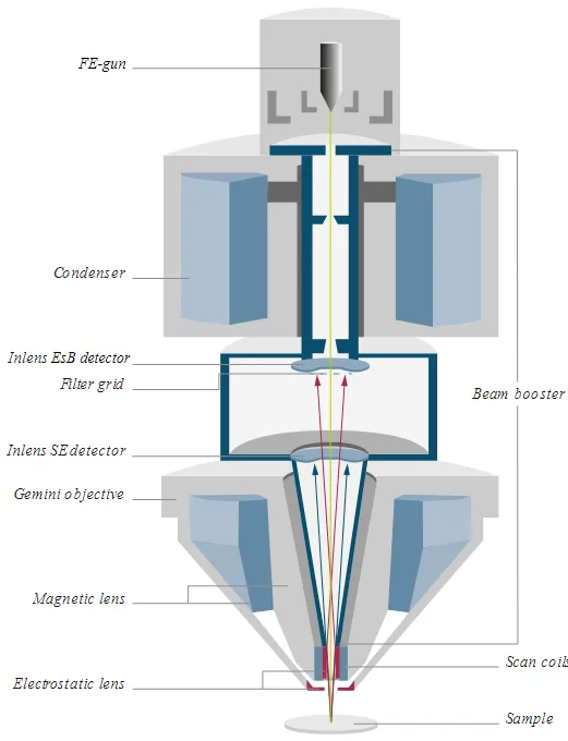
Gemini optics are characterized by three main components:
- The Gemini objective lens design combines electrostatic and magnetic fields to maximize optical performance while reducing field influences at the sample to a minimum. This enables excellent imaging, even on challenging samples such as magnetic materials.
- Gemini beam booster technology, an integrated beam deceleration, guarantees small probe sizes and high signal-to-noise ratios.
- The Gemini Inlens detection concept ensures efficient signal detection by detecting secondary (SE) and backscattered (BSE) electrons in parallel minimizing time-to-image.
For your applications benefit from:
- Long-term stability of the SEM alignment and the effortless way it adjusts all system parameters such as probe current and acceleration voltage.
- Achieve distortion-free, high resolution imaging with the help of the near magnetic-field free optics.
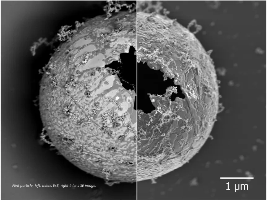
- Get information solely from the top-most layer of your samples with the Inlens SE detector that produces images out of the truly surface sensitive SE 1 electrons.
- Obtain true material contrast at very low voltages with the detection concept of the Inlens EsB detector.
Gemini 2
Capitalize on Fast Analytics
A comprehensive characterization of any sample calls for performance in imaging and in analytics. Plus, today’s users expect the set up and handling of the instrument to be easy. The Gemini 2 optics answers these demands
Switch seamlessly between high resolution imaging and analytics
- GeminiSEM 460 comes with Gemini 2 optics featuring a double condenser.
- Adjust the beam current continuously while the spot size stays optimized simultaneously.
- Switch seamlessly between high resolution imaging – at low beam currents – and analytical modes – at high beam currents.
- You save time and effort because there’s no need to realign the beam after changing imaging parameters.

Stay flexible and work efficiently
- Stay flexible: use the highest beam current density for high resolution imaging and analysis at both low and high beam current, independently of which beam energy you select.
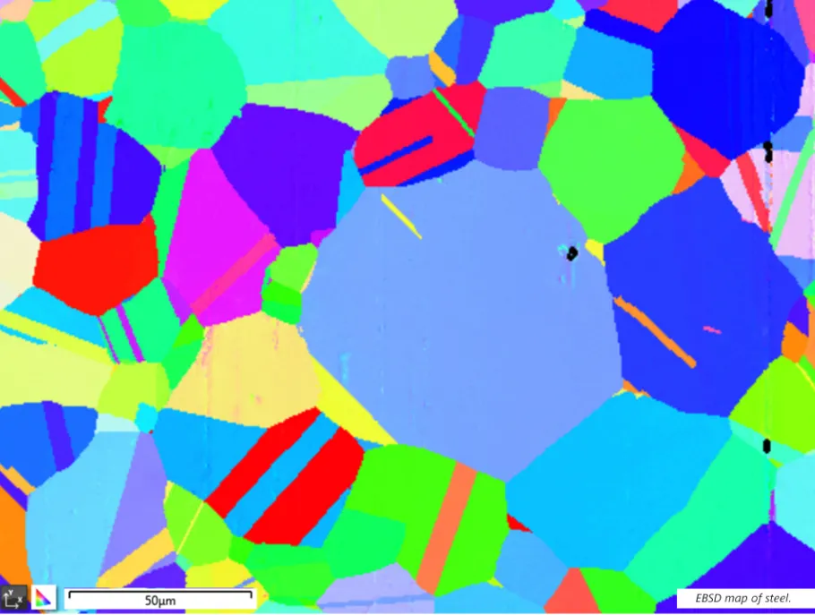
- Your specimen won’t be exposed to a magnetic field: achieve distortion-free EBSD patterns and high resolution imaging over a large field of view.
- Tilt the specimen without influencing the electron optical performance. Image even magnetic samples easily.
- Choose a charge reduction mode that suits your sample best: local charge compensation, variable pressure in the chamber or NanoVP.
Gemini 3
Imaging below 1 kV - Expert Knowledge Integrated
The Gemini 3 optics are optimized for resolutions at low and very low voltages, and for contrast enhancement. They ensure maximum resolution at all working conditions from 1 kV to 30 kV and consists of two components which work synergistically: the Nano-twin lens and Smart Autopilot, a new electron optical engine. Additional technological characteristics are the high gun resolution mode and the optional Tandem decel.
Resolution Modes – Enabling You to See More Details
More details and more detection signal for your SEM images, enabled by two modes. In high resolution gun mode, the reduced energy spread of the primary beam minimizes the effect of chromatic aberration to allow even smaller probe sizes. In Tandem decel mode, a deceleration voltage is applied to the sample. Use this to further improve resolution below 1 kV and boost the detection efficiency of backscattered diode detectors.
The Nano-twin lens delivers:
- Sub-nanometer resolution at low and ultra-low voltages with excellent signal detection efficiency.
- Three times lower lens aberrations at low kV compared to the standard Gemini objective lens - resulting in a three times lower magnetic field on the sample, of the order of 1 mT.
- Optimized geometry and the electrostatic and magnetic field distributions.
- An enhanced Inlens detector signal under low voltage imaging conditions.
- These characteristics provide the ability for sub-nanometer imaging below 1 kV without immersing the sample in an electro-magnetic field.
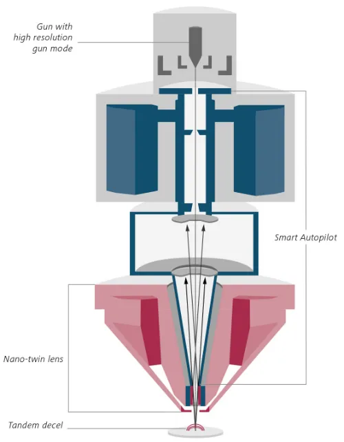
How it works:
- Smart Autopilot optimizes electron trajectories through the column thus ensuring the highest possible resolution at each acceleration voltage.
- The autofunctions enable a seamless alignment free transition across the entire magnification range from 1× to 2,000,000× and a 10× increase in the field of view allowing a 13 cm object to be imaged in a single frame.
- The image framestore of 32k × 24k in combination with the new overview mode ensure a stitching free pixel density over an unparalleled field of view
Applications in Materials Science
Typical Tasks and Applications
- Image and analyze any real-world sample effortlessly, over large areas or at sub-nanometer resolution.
- Explore examples from nanoscience, engineering and energy materials, or bio-inspired materials, polymers & catalysts.
- See how GeminiSEM helps you to characterize your specimen comprehensively.
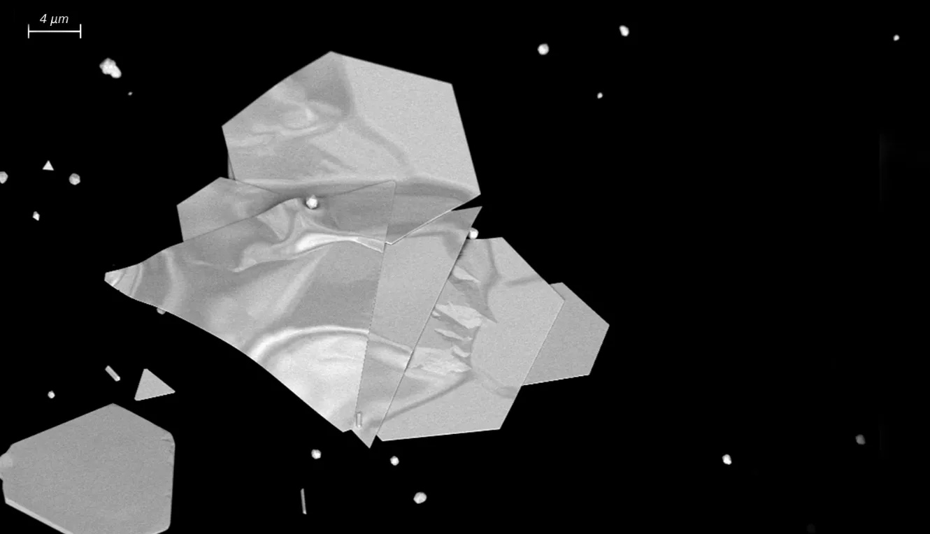
Caption: Structured gold platelets, research on plasmonic effects, GeminiSEM 560, BSD.
Microscopy Solutions for Industry
Typical Tasks and Applications
- Failure analysis on mechanical, optical or electronic components
- Fracture analysis and metallography
- Surface, microstructure and device characterization
- Compositional and phase distribution
- Impurity and inclusion determination
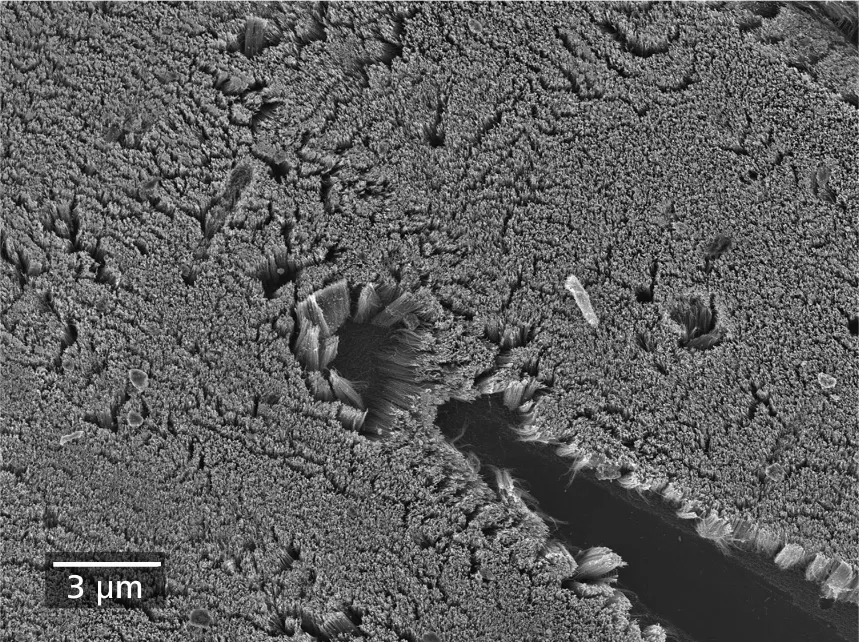
Caption: Cross-section of lithium ion battery

Applications in Electronics & Semiconductor
Typical Tasks and Applications
- Construction analysis and benchmarking
- Passive voltage contrast
- Subsurface analysis
- Electronic property measurement with probing
- TEM site selection
Caption: The aBSD detector at high EHT (here at 30 kV ) shows deeply-buried structures such as FinFET gates, tungsten plugs, and tin liner (inset) with exceptional resolution and contrast.

Applications in Life Sciences
Applications in Life Sciences
- Characterization of topology
- Imaging sensitive, non-conductive, outgassing, or low contrast samples
- Visualizing the ultrastructure of cells, tissues etc. at high resolutions
- Imaging very large areas such as serial sections or block faces
Caption: SARS-CoV-2 virus, culture, inactivated, negatively stained, GeminiSEM 560, aSTEM, HAADF/BF.

